上面図
このセクションでは、ソリューションの上面図について説明します。
図 1. 計算ノードの上面図
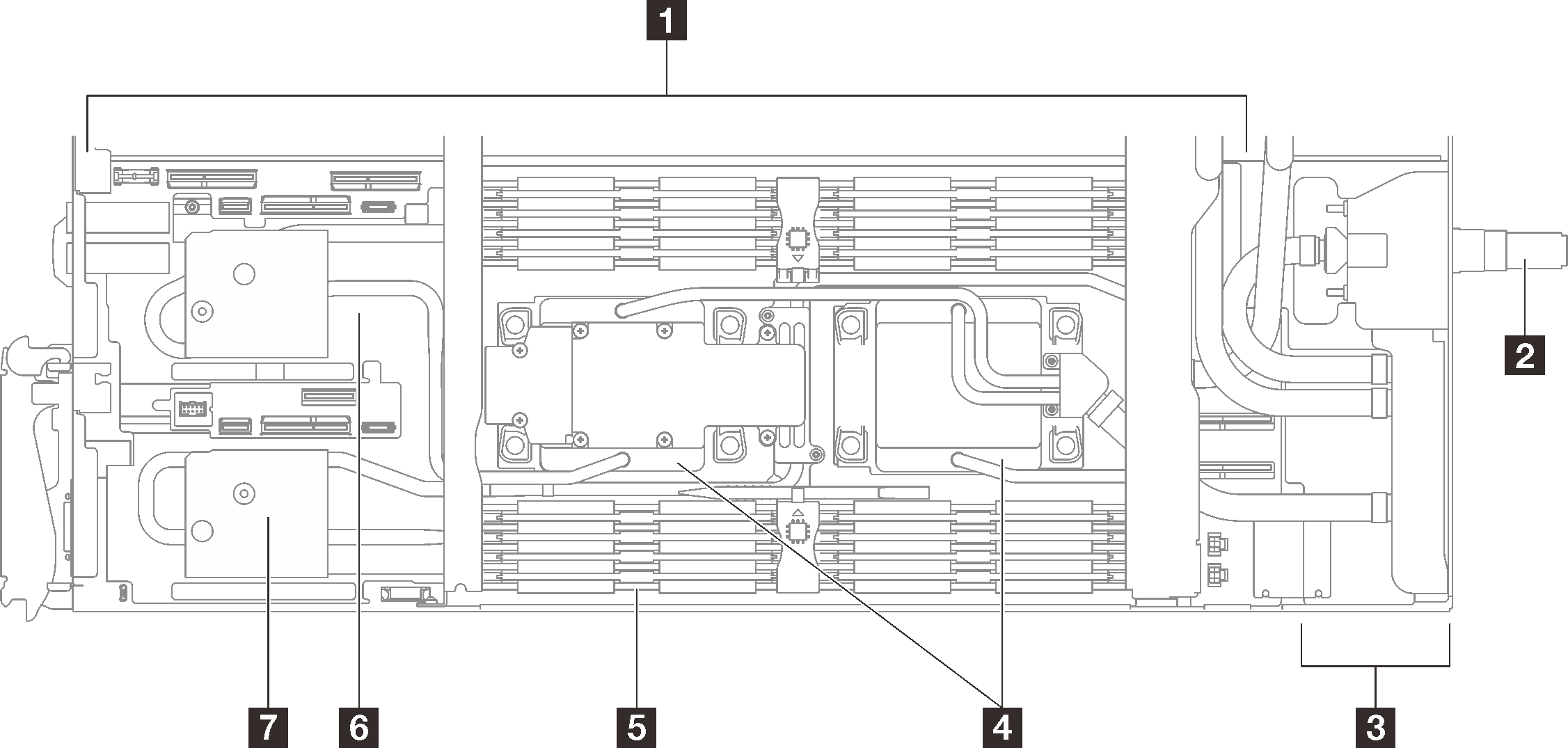
| 1 システム・ボード | 5 メモリー・モジュールのコールド・プレート |
| 2 ウォーター・ループ・クイック・コネクト | 6 PCIe 5.0 x16 スロット 2 またはドライブ・ベイ 0/1 |
| 3 分電盤 | 7 PCIe 5.0 x16 スロット 1 またはドライブ・ベイ 2/3 |
| 4 プロセッサー・コールド・プレート |
図 2. GPU ノードの上部図
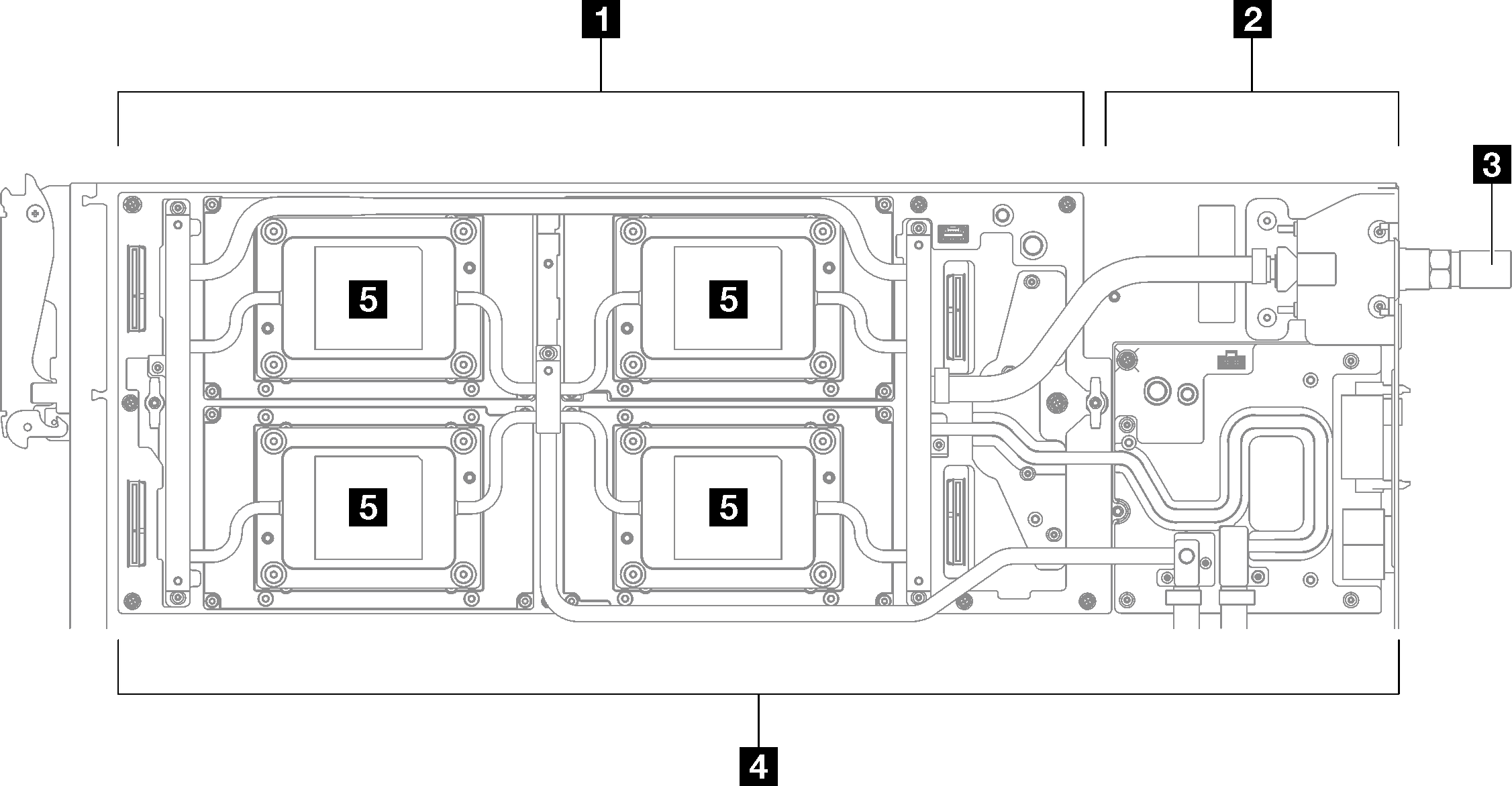
| 1 キャリア・ベース・ボード (CBB) | 4 ウォーター・ループ |
| 2 分電盤 | 5 GPU OAM コールド・プレート |
| 3 ウォーター・ループ・クイック・コネクト |
フィードバックを送る