Gap pad/Putty pad identification and location
Follow the information in this section to identify their shape, location, and orientation of the various gap pads and putty pads used in SD665-N V3.
Installation Guidelines for gap pad and putty pad
For the gap pad and putty pad used in SD665-N V3, see the following sections:
Attention
There are two types of thermal pad: putty pad and gap pad.
Gap pad—Replace gap pad if it is damaged or missing.
Putty pad— When replacing components, always replace putty pads with new ones.
Do not use expired putty pad. Check the expiry date on putty pad package. If the putty pads are expired, acquire new ones to properly replace them.
Water loop and GPU node — Gap pad/Putty pad identification and location
Figure 1. Water loop and GPU node — Gap pad/Putty pad identification and location
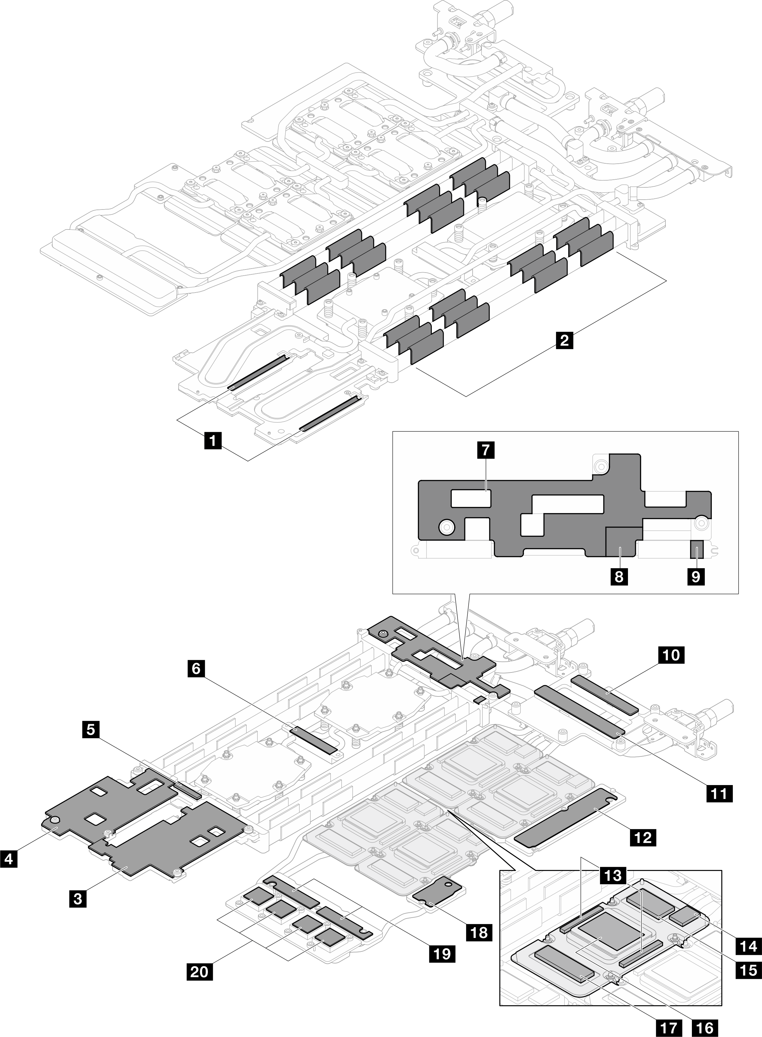
| Pad index | Pad type | Attached component | Pad orientation |
|---|---|---|---|
| 1 | Gap pad | Compute node water loop | Gray side facing outward |
| 2 | Gap pad | Compute node water loop | Gray side facing outward |
| 3 | Gap pad | Compute node water loop | Gray side facing outward |
| 4 | Putty pad | Compute node water loop | Both sides can be facing outward |
| 5 | Putty pad | Compute node water loop | Both sides can be facing outward |
| 6 | Gap pad | Compute node water loop | Gray side facing outward |
| 7 | Gap pad | Compute node water loop | Gray side facing outward |
| 8 | Gap pad | Compute node water loop | Gray side facing outward |
| 9 | Putty pad | GPU node water loop | Both sides can be facing outward |
| 10 | Putty pad | GPU node water loop | Both sides can be facing outward |
| 11 | Putty pad | GPU node water loop | Align pad cutout to the screw hole and opening on the water loop |
| 12 | Putty pad | GPU | Both sides can be facing outward |
| 13 | Putty pad | GPU | Both sides can be facing outward |
| 14 | Putty pad | GPU | Both sides can be facing outward |
| 15 | Phase change material (PCM) | GPU node water loop | Both sides can be facing outward Note A PCM jig is required for installing the PCM to GPU node water loop. |
| 16 | Putty pad | GPU | Both sides can be facing outward |
| 17 | Putty pad | GPU node water loop | Both sides can be facing outward |
| 18 | Putty pad | GPU node water loop | Align pad cutout to the screw hole and opening on the water loop |
| 19 | Putty pad | GPU node water loop | Both sides can be facing outward |
Compute node components — Gap pad/Putty pad identification and location
| Pad index | Pad type | Attached component | Pad orientation |
|---|---|---|---|
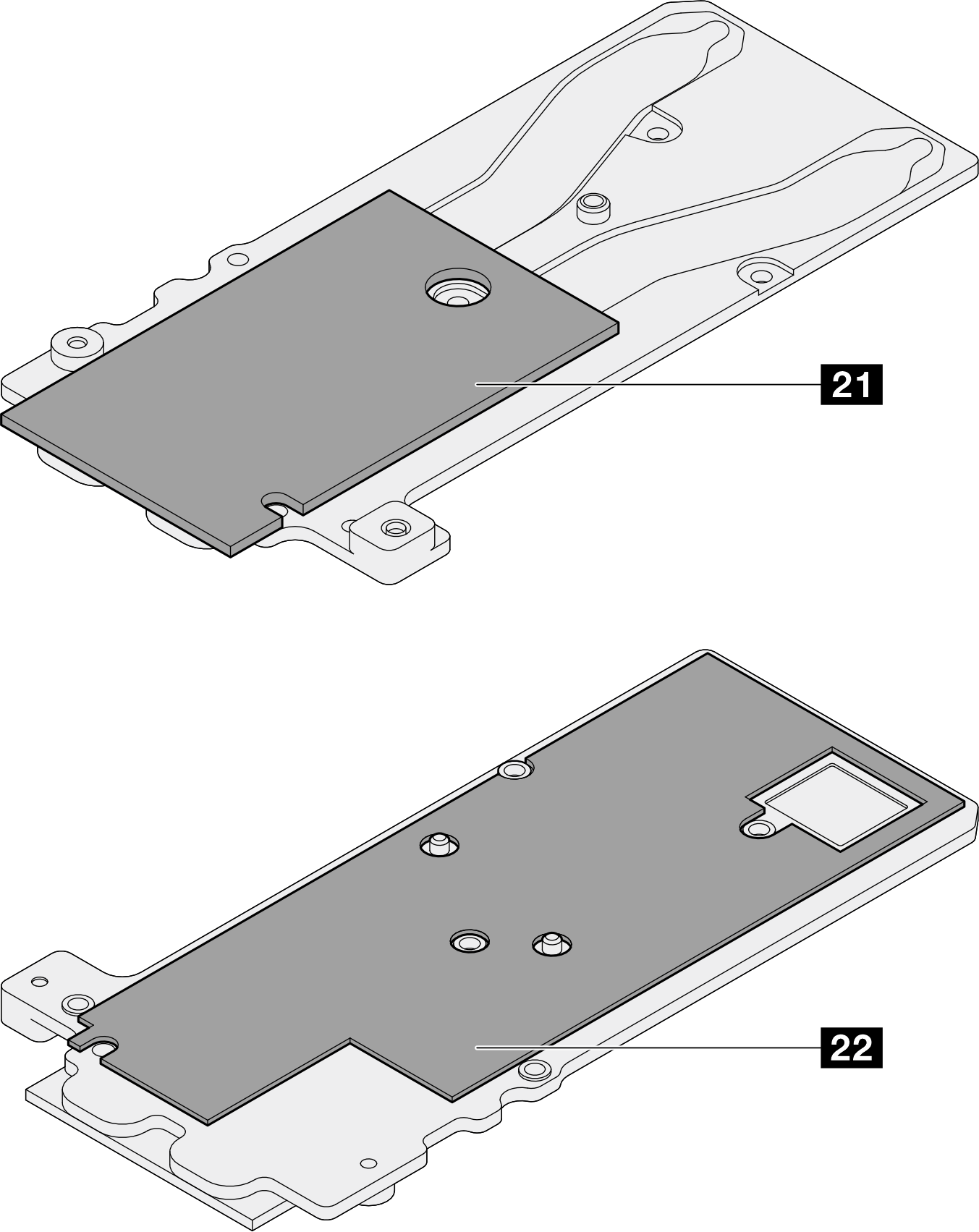
| 20 | Putty pad | OSFP module conduction plate | Align pad cutout to the screw hole and opening on the interface plate as shown in: |
| 21 | Putty pad | OSFP module conduction plate | |
| 22 | Putty pad | M.2 backplane assembly | Align pad cutout to the screw hole and opening on the interface plate as shown in Install an M.2 drive. |
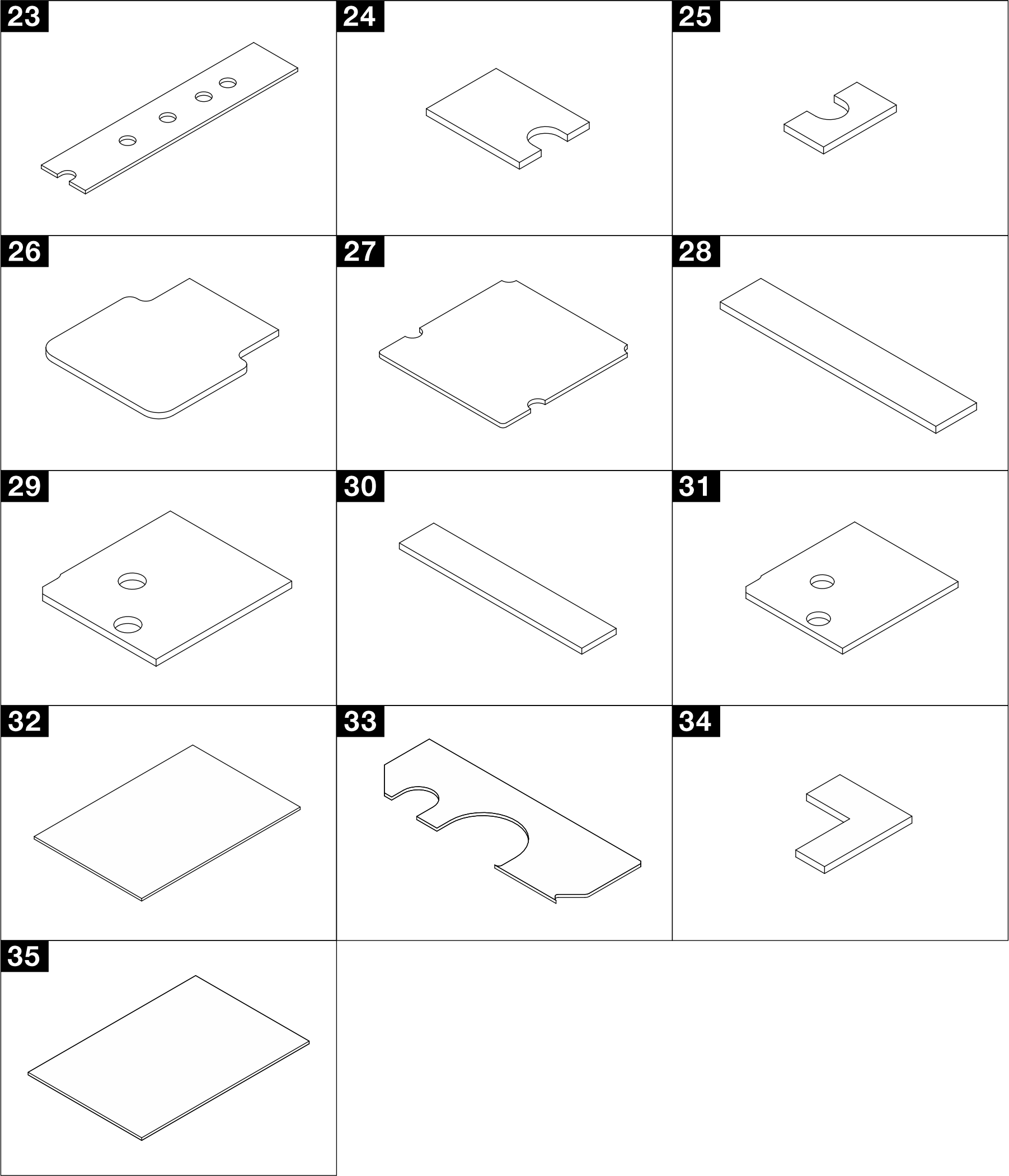
| 23 | Putty pad | M.2 backplane assembly | Align pad cutout to the screw hole and opening on the interface plate as shown in Install the M.2 backplane assembly. |
| 24 | Putty pad | M.2 backplane assembly | |
| 25 | Putty pad | M.2 backplane assembly | |
| 26 | Putty pad | M.2 backplane assembly | |
| 27 | Gap pad | Conduction plate for:
| Gray side facing outward |
| 28 | Gap pad | Drive cage for:
| Align pad cutout to the screw hole and opening on the interface plate as shown in Install a drive cage assembly |
| 29 | Putty pad | Conduction for U.3 7mm drive | Both sides can be facing outward |
| 30 | Gap pad | Drive cage for U.3 7mm drive | Align pad cutout to the screw hole and opening on the interface plate as shown in Install a drive cage assembly |
| 31 | Gap pad | E3.S drive conduction plate | Apply the adhesive side to the E3.S drive conduction plate, see Install an E3.s drive |
| 32 | Putty pad | Align pad cutout to the screw hole and opening on the interface plate as shown in Install an E3.s drive | |
| 33 | Putty pad | ||
| 34 | Gap pad | E3.S drive cage | Apply the adhesive side to the water loop. |
| Pad index |
|---|
35 VR 2.5 mm Putty Pad
|
36 VR 1.5mm Putty Pad
|
Give documentation feedback