Install a memory module
The following notes describe the types of DIMMs that the node supports and other information that you must consider when you install DIMMs.
See Memory module installation order for detailed information about memory configuration and setup.
- Confirm that the node supports the DIMM that you are installing (see Lenovo ServerProven website).
- When you install or remove DIMMs, the node configuration information changes. When you restart the node, the system displays a message that indicates that the memory configuration has changed. You can use the Setup utility to view the node configuration information, see System configuration for more information.
- Install higher capacity (ranked) DIMMs first, following the population sequence for the Memory Mode being used.
- The node supports only industry-standard double-data-rate 4 (DDR4), 2666 MT/s, PC4-21300 (single-rank or dual-rank), unbuffered or synchronous dynamic random-access memory (SDRAM) dual inline memory modules (DIMMs) with error correcting code (ECC).
Do not mix RDIMMs, LRDIMMs and 3DS DIMMs in the same node.
- The maximum operating speed of the node is determined by the slowest DIMM in the node.
- If you install a pair of DIMMs in DIMM connectors 1 and 3, the size and speed of the DIMMs that you install in DIMM connectors 1 and 3 must match each other. However, they do not have to be the same size and speed as the DIMMs that are installed in DIMM connectors 2 and 4.
- You can use compatible DIMMs from various manufacturers in the same pair.
- The specifications of a DDR4 DIMM are on a label on the DIMM, in the following format.
gggGBpheRxff PC4-wwwwaa-mccd-bb
where:- gggGB is the total capacity, in gigabytes, for primary bus (ECC not counted) 4GB, 8GB, 16GB, etc. (no space between digits and units)
- pheR is the number of package ranks of memory installed and number of logical ranks per package rank
- p =
- 1 = 1 package rank of SDRAMs installed
- 2 = 2 package ranks of SDRAMs installed
- 3 = 3 package ranks of SDRAMs installed
- 4 = 4 package ranks of SDRAMs installed
- he = blank for monolithic DRAMs, else for modules using stacked DRAM:
- h = DRAM package type
- D = multi-load DRAM stacking (DDP)
- Q = multi-load DRAM stacking (QDP)
- S = single load DRAM stacking (3DS)
- e = blank for SDP, DDP and QDP, else modules using 3DS stacks, logical ranks per package rank
- 2 = 2 logical ranks in each package rank
- 4 = 4 logical ranks in each package rank
- 8 = 8 logical ranks in each package rank
- h = DRAM package type
- R = rank(s)
- xff = Device organization (data bit width) of SDRAMs used on this assembly
- x4 = x4 organization (4 DQ lines per SDRAM)
- x8 = x8 organization
- x16 = x16 organization
- p =
- wwwww is the DIMM bandwidth, in MBps: 2133, 2400, 2666, 2933, 3200
- aa is the SDRAM speed grade
- m is the DIMM type
- E = Unbuffered DIMM (UDIMM), x64 primary + 8 bit ECC module data bus
- L = Load Reduced DIMM (LRDIMM), x64 primary + 8 bit ECC module data bus
- R = Registered DIMM (RDIMM), x64 primary + 8 bit ECC module data bus
- U = Unbuffered DIMM (UDIMM) with no ECC (x64-bit primary data bus)
- cc is the reference design file used for this design
- d is the revision number of the reference design used
- bb is the JEDEC SPD Revision Encoding and Additions level used on this DIMM
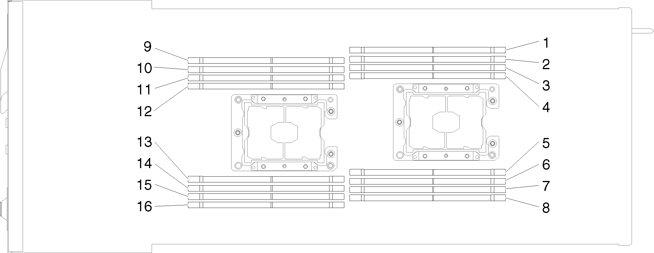
The following illustration shows the location of the DIMM connectors on the system board.
Figure 1. The location of the DIMM connectors on the system board
Give documentation feedback